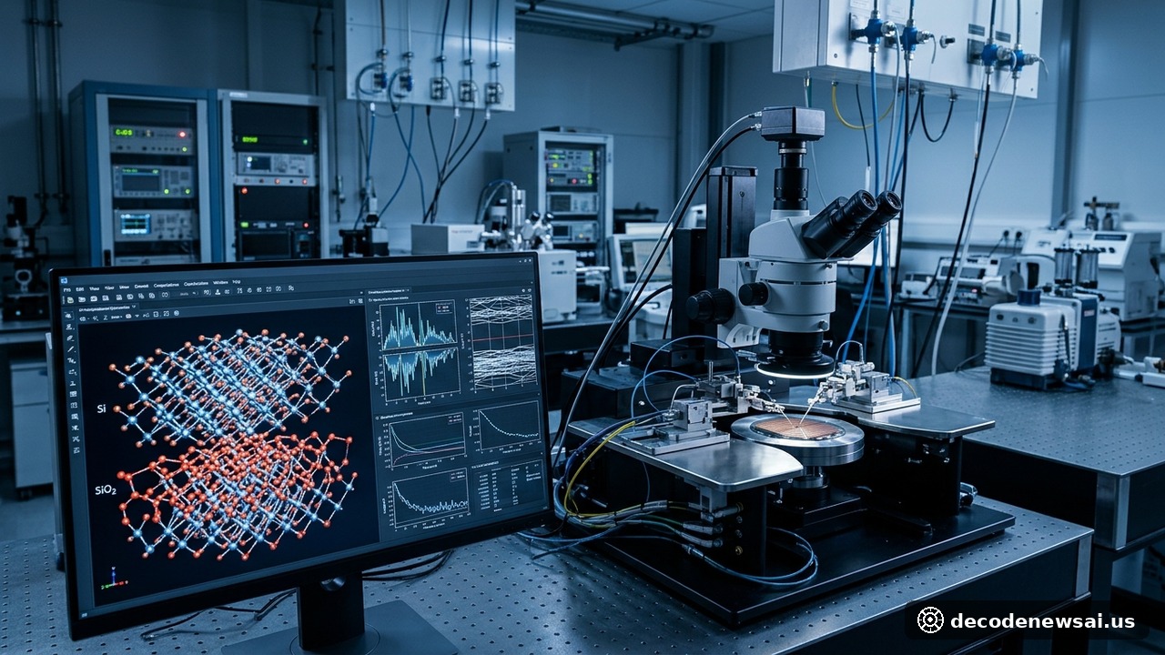
San Francisco-based artificial intelligence startup Discovered Materials, a graduate of Y Combinator's spring 2026 cohort specializing in generative physics for semiconductor materials discovery, officially launched a $1 million grand challenge prize pool on November 5, 2026, offering $200,000 for each validated solution to five fundamental, unsolved problems in condensed matter physics and materials science. According to technical benchmarking documentation released alongside the launch, the company rigorously evaluated current frontier laboratory AI models—providing autonomous agents with persistent computational resources and internet access across multi-day evaluation trials—and observed zero meaningful progress across any of the five challenges, demonstrating the severe limitations of current reasoning models when applied to non-deterministic physical systems.
What Are the Quantifiable Prize Metrics and Engineering Milestones of the Discovered Materials Challenge?
- Duration of Autonomous Frontier AI Pre-Tests: Multiple Continuous Days (Zero Meaningful Breakthroughs)
- Founder's Projected Timeline to Useful Material Discovery: Sub-12-Month Horizon Following August 2026 Seed Round
In detailed interviews with TechCrunch and Emergent, Discovered Materials co-founder and Chief Executive Officer Advaith Sridhar emphasized that while frontier AI models have demonstrated extraordinary breakthroughs in abstract mathematics and macromolecular biology, generative materials science has long been hindered by a lack of rigorous, verifiable evaluation benchmarks. Unlike competitive programming or mathematical theorem proving—where solutions can be autonomously compiled or formally verified—materials science problems require empirical physical validation. By collaborating with leading academic institutions to formalize precise mathematical and computational success criteria, the startup is creating the first standardized benchmarking framework for physical AI reasoning.
The five grand challenges were formulated in close consultation with materials science faculties from Stanford University, the University of Cambridge, and the Interuniversity Microelectronics Centre (IMEC).
What Specific Semiconductor Physical Bottlenecks Do the Five Open Challenges Target?
The challenge focuses on intractable physical phenomena that directly constrain next-generation semiconductor fabrication, quantum computing, and thermal dissipation architectures.
The first problem demands a comprehensive theoretical framework capable of explaining high-temperature cuprate superconductivity to enable room-temperature energy transmission. The second challenge requires an accurate numerical methodology to predict structural interfaces between silicon and silicon dioxide (Si-SiO2), a boundary condition essential for halting quantum tunneling leakage in sub-2nm transistor architectures. The third problem targets mapping poly-crystalline grain morphology to macroscopic thermal conductivity, directly addressing thermal throttling in ultra-dense AI accelerator packages. The fourth challenge seeks to model light-induced phase shifts in electronic materials, while the fifth demands structural mathematical improvements to Density Functional Theory (DFT) algorithms, significantly reducing computational overhead in quantum-mechanical modeling.
Academic researchers involved in defining the five grand challenges noted that current large language models struggle when reasoning across multiscale physical phenomena. While neural networks excel at synthesizing existing scientific literature or generating molecular candidates with similar topological features, solving unsolved condensed matter physics problems requires discovering novel mathematical formulations that cannot be interpolated from training data.
By establishing open verification frameworks that provide objective truth criteria, the challenge aims to redirect AI research toward rigorous fundamental science. Winning solutions will undergo comprehensive experimental peer review and independent replication in specialized fabrication laboratories before prize disbursements are finalized. This rigorous verification standard ensures that rewarded breakthroughs deliver immediate technological value to commercial semiconductor manufacturers worldwide.
What Strategic Repercussions Does This Challenge Hold for Frontier AI and Chip Fabrication?
Discovered Materials' $1 million initiative marks an inflection point in artificial intelligence research, compelling developers to pivot from stochastic pattern recognition toward rigorous ground-truth scientific derivation.
For leading semiconductor manufacturing consortiums, conventional trial-and-error laboratory synthesis has reached unsustainable cost curves as transistor architectures approach atomic tolerances. By establishing unambiguous targets and open verification pipelines, the initiative accelerates the advent of autonomous AI scientist systems capable of designing novel low-k dielectrics, ultra-wide bandgap substrates, and advanced thermal interface compounds, catalyzing an epochal paradigm shift across advanced electronic materials manufacturing.