What Are the Key Benchmark Scores and Architectural Parameters in the Leak?
- Geekbench 7 Multi-Core Score: 18,313 Points
- Leaked Sample Physical Core Count: 10 Cores Identified (Final SKU up to 12)
System metadata extracted from the benchmark repository indicates that the test run was executed on a prototype validation motherboard manufactured by Lenovo for prospective thin-and-light professional laptops. While the pre-silicon test unit was operating with only 10 cores enabled and lacked finalized dynamic boost firmware, the architecture exhibited remarkable instruction-per-clock (IPC) execution capabilities. Compared to the preceding Zen 5 design, Zen 6 introduces extensive pipeline widening, overhauled branch prediction algorithms, and enhanced dual-ported load-store units designed to accelerate single-threaded software execution.
Semiconductor analysts observed that achieving 3,100 single-core points on pre-release hardware indicates that production silicon, once tuned for commercial maximum turbo frequencies, will easily outpace current desktop benchmarks. The results demonstrate that AMD's architectural team has successfully decoupled extreme single-thread performance from heavy thermal envelopes, providing notebook designs with workstation-grade compute density.
The benchmark logs also revealed enhanced memory controller responsiveness, suggesting that Medusa Point incorporates dedicated low-power LPDDR5X-9600 memory channels alongside early validation for high-speed PCIe 6.0 interconnect lanes. The integration of high-bandwidth memory interfaces directly addresses the data-transfer bottlenecks that have traditionally throttled integrated graphics and neural processing execution on high-end laptops.
What Advantages Do TSMC's 2nm Node and Advanced Chiplet Packaging Provide?
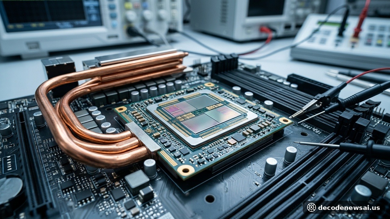
The Medusa Point processor represents AMD's commercial transition to TSMC's 2-nanometer (N2) production node, which replaces traditional FinFET designs with Gate-All-Around (GAA) nanosheet transistors. The structural shift reduces parasitical capacitance, curtails gate leakage current, and delivers a notable improvement in energy efficiency at mobile thermal design points between 28 and 54 watts.
By stacking cache dies directly atop computing logic using third-generation hybrid bonding techniques, AMD achieved a 30% reduction in chiplet footprint compared to equivalent Zen 5 packaging. This compact physical form factor enables laptop manufacturers to design sleeker thermal chassis without compromising board space for extended battery modules.
How Will the Benchmark Emergence Impact Desktop and Data Center Competition?
The benchmark appearance arrives at a sensitive moment for competing chipmaker Intel Corporation, which has spent recent quarters marketing its Lunar Lake low-power platforms and Arrow Lake performance processors to commercial laptop partners. Demonstrating superior single-core performance on early, throttled Zen 6 test silicon establishes an intimidating technological threshold for original equipment manufacturers planning product roadmaps for 2027.
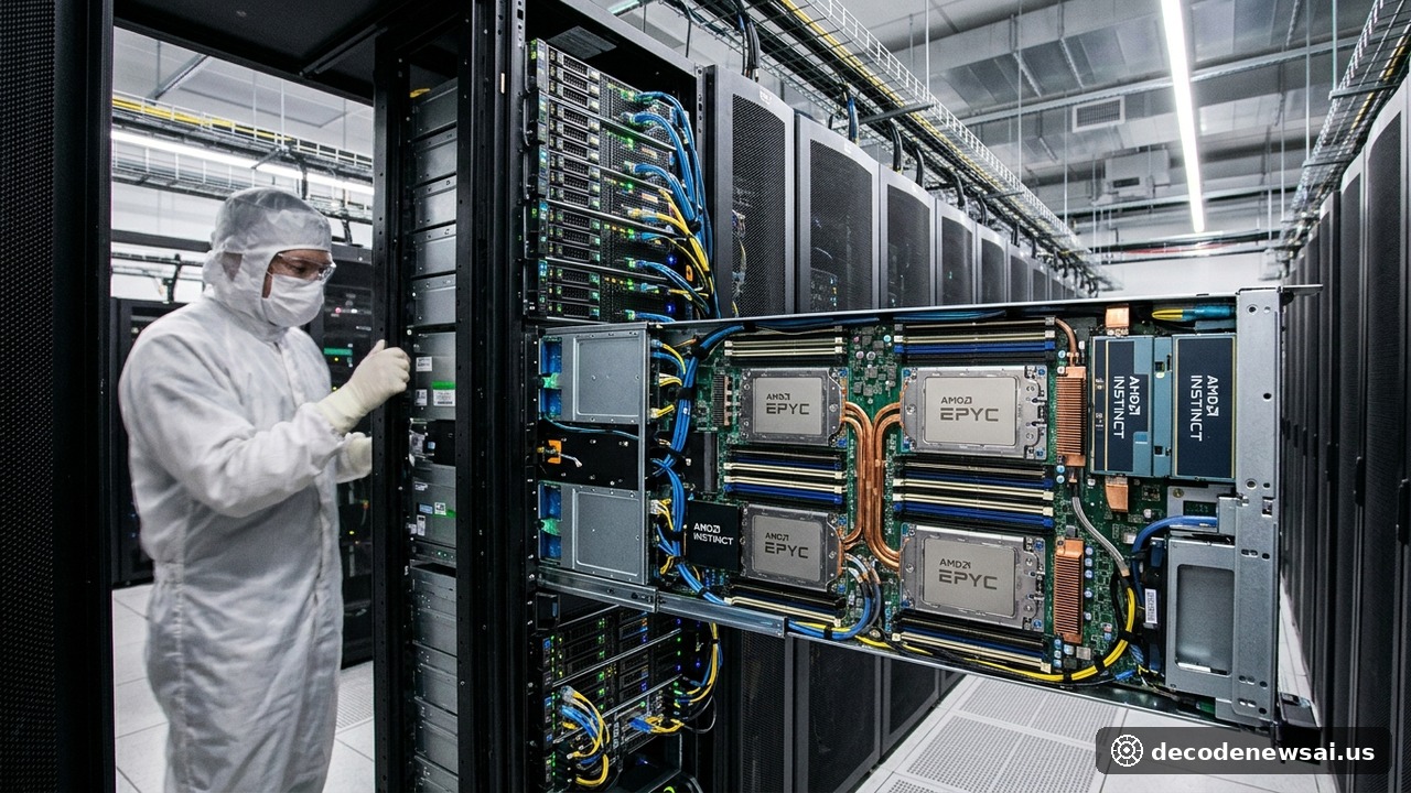
Although AMD chief executive officer Lisa Su emphasized during recent investor discussions that enterprise data center acceleration remains the corporate priority, the underlying microarchitectural advances demonstrated in Medusa Point directly inform server silicon. The fundamental execution engine refined in Medusa Point will serve as the computing core for AMD's future Venice-generation EPYC server chips, positioning the company to preserve its momentum against hyperscale rival architectures.
In terms of competitive positioning, the emergence of Medusa Point demonstrates that AMD's multi-generational commitment to modular chiplet topologies is paying substantial dividends against monolithic die approaches. By disaggregating high-performance CPU cores, low-power system management silicon, and scalable AI accelerators across separate optimized process nodes, AMD can maximize wafer yield while curtailing packaging expenses. Commercial hardware partners anticipate that finalized Zen 6 silicon will establish the standard for high-performance AI PCs throughout the late 2020s.