Key Operational Metrics: Semiconductor Foundry Allocation and Enterprise AI Revenue
- Nvidia Next-Gen HBM Controller Process: Custom TSMC 3nm Enhanced Architecture;24/7 Wall St. Semiconductor Review
- Automotive & Industrial Edge Computing: $1.06 Billion USD (Sixth Straight Qtr Growth)
- HBM4 Interconnect Throughput Density: 2.2x Density Gain (Exceeding 2 TB/s Bandwidth)
- Global Data Center AI Inference Market: Projected to Surpass $85 Billion by 2027
Why Did TSMC Secure Exclusive Manufacturing Rights for Nvidia's Next-Gen HBM?
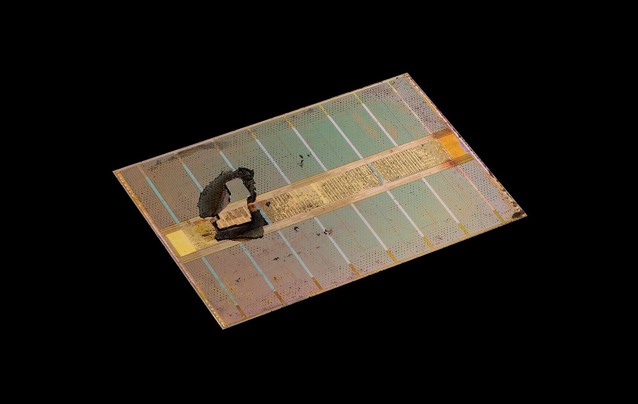
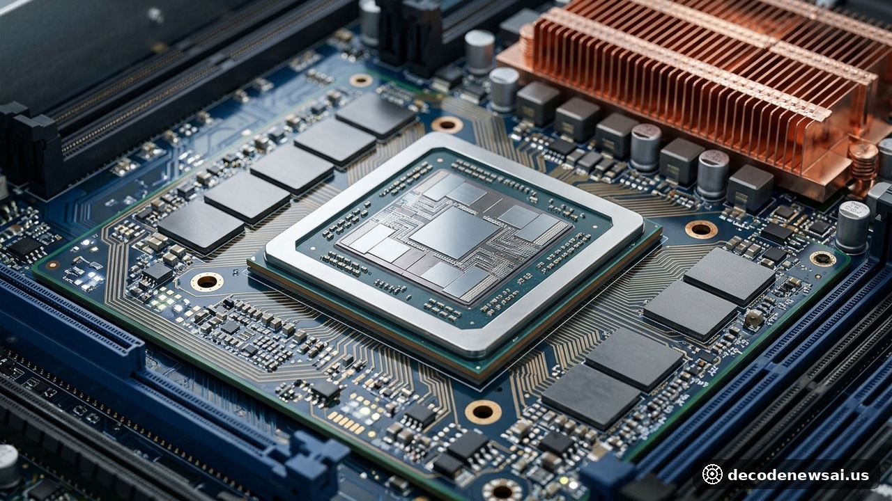
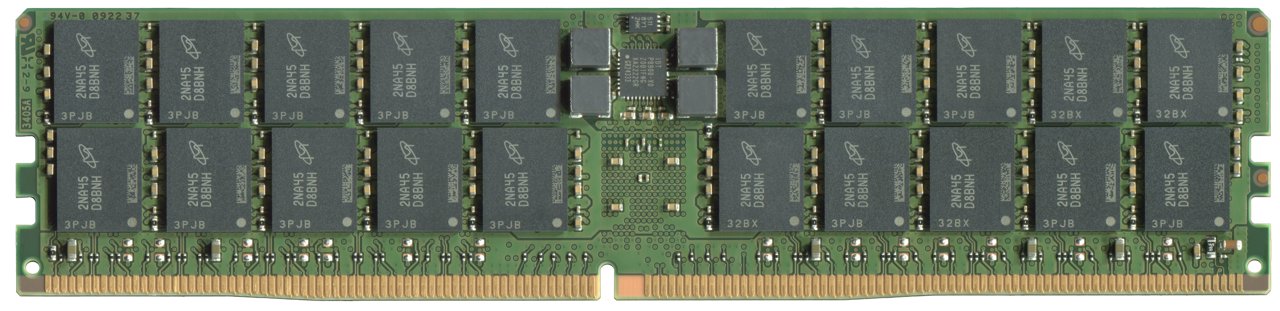
Nvidia's architectural requirements for its upcoming Rubin platform represent a departure from previous GPU design paradigms, placing unprecedented demands on memory bandwidth density and low-latency packaging interconnects. Under previous HBM3e specifications, the underlying memory base die relied on conventional logic processing. However, HBM4 architecture dictates that the base controller die must be directly fabricated on cutting-edge sub-5nm logic process nodes to facilitate dense 3D vertical stacking directly adjacent to the primary compute accelerators.
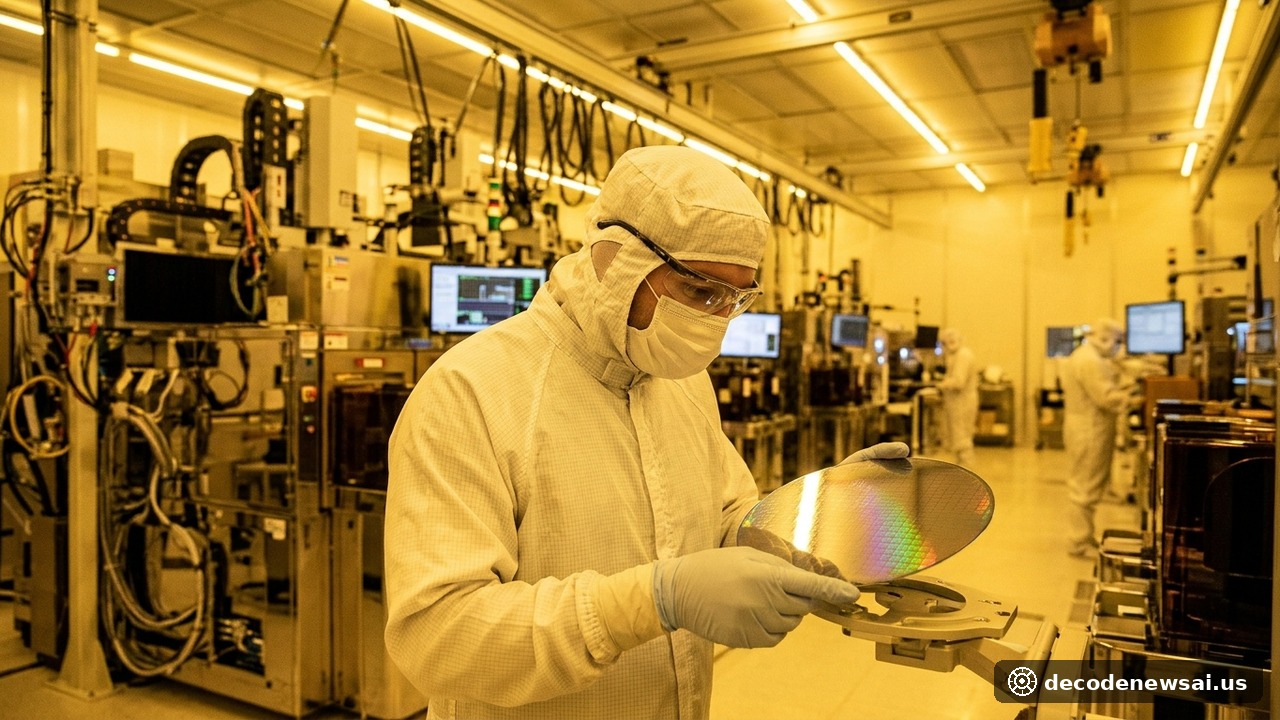
TSMC leveraged its mature, commercially proven Chip-on-Wafer-on-Substrate (CoWoS) and System-on-Integrated-Chips (SoIC) advanced packaging ecosystems to secure the entire contract. TSMC's microelectronics engineering team developed a specialized 3nm low-power logic interface tailored specifically for Nvidia's proprietary NVLink crossbar architecture. This implementation achieves bidirectional memory bandwidth exceeding 2 terabytes per second while reducing dynamic power consumption by 30% compared to competing multi-chip packaging methods. This exclusive engagement secures high-margin fab capacity for TSMC through the remainder of the decade, cementing its dominance across the physical hardware foundation of enterprise artificial intelligence.
What Does Qualcomm's $10.4 Billion Quarter Mean for Enterprise AI Diversification?
Long regarded primarily as a provider of cellular modems and consumer smartphone application processors, Qualcomm's fiscal 2026 performance demonstrates that its corporate diversification agenda is yielding structural returns. Fourth-quarter revenue of $10.44 billion surpassed consensus equity estimates, propelled by double-digit growth across automotive digital chassis installations and enterprise cloud compute modules.
Significantly, Qualcomm is successfully establishing a foothold within hyperscale cloud data centers. Utilizing custom ARM-based Oryon CPU cores originally developed through its Nuvia acquisition, Qualcomm launched dedicated cloud inference acceleration cards that prioritize electrical efficiency and total cost of ownership (TCO). As global cloud service providers grapple with massive electrical grid constraints and surging cooling overhead, Qualcomm's high-efficiency silicon has secured multi-megawatt pilot deployments across major North American cloud operators, providing the company with an enduring commercial growth vector outside of consumer electronics.
How Are Semiconductor Giants Navigating Advanced Packaging and Heterogeneous Compute?
The corporate strategies executed by Nvidia, TSMC, and Qualcomm highlight a transformative shift in semiconductor engineering: the transition away from monolithic planar scaling toward heterogeneous multi-die co-packaging and system-level thermal co-design. As physical atomic limitations constrain traditional Dennard scaling, commercial competition between TSMC, Intel Foundry, and Samsung Electronics is increasingly contested across advanced multi-die packaging, silicon photonics optical interconnects, and substrate microfluidic cooling channels.
Semiconductor industry analysts note that the proliferation of reasoning-centric frontier models is fundamentally altering compute hardware economics. The imperative to break through the memory wall and communications interconnect bottlenecks requires comprehensive vertical integration across silicon fabs, memory producers, and system architects. Whether anchored by TSMC's advanced wafer-level packaging or Qualcomm's power-efficient distributed inference modules, the microelectronics sector is entering an unprecedented era of architectural innovation and capital expenditure.