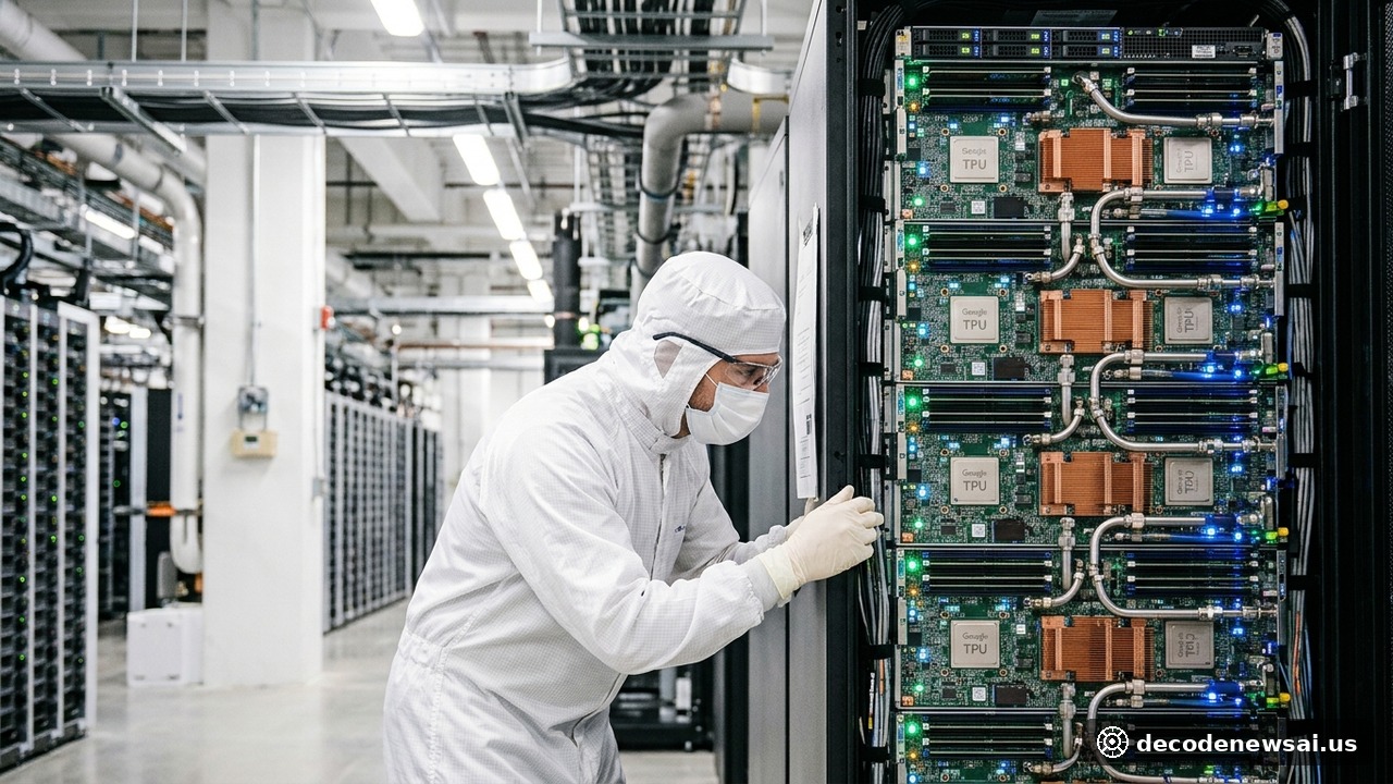
MOUNTAIN VIEW, Calif. - Alphabet subsidiary Google officially announced two new accelerator systems on Monday, November 9. It expanded its eighth-generation Tensor Processing Unit portfolio. The unveiling covered the TPU 8tx and TPU 8i Max. The dual-chip expansion is the first time Google has introduced four specialized TPU systems within a single calendar year. It advances its custom silicon challenge against merchant GPU accelerators.
TPU 8tx adds hardware-enforced confidential computing
The TPU 8tx is Google's first specialized accelerator with hardware-enforced confidential computing. The architecture puts hardware-level memory encryption engines directly into the silicon boundary. Sensitive model weights and customer inference data stay cryptographically isolated and encrypted while in flight across memory channels. The capability removes vulnerabilities tied to physical side-channel memory inspections.
Confidential compute features address compliance barriers that have restricted enterprise AI adoption in highly regulated environments. Commercial entities in algorithmic trading, patient healthcare diagnostics, and national defense previously faced legal prohibitions. Those rules barred transmitting proprietary datasets to multi-tenant hyperscale cloud facilities. TPU 8tx provides cryptographically verified isolation within shared Google Cloud infrastructure.
Google's Chief Technologist for AI and Infrastructure stated in the official announcement: 'TPU 8tx and TPU 8i Max provide dedicated architectural specialization for the agentic era, combining hardware-enforced confidential computing with unprecedented scale.' Semiconductor engineers commended the silicon design.
TPU 8i Max doubles memory for agentic workflows
The companion TPU 8i Max system addresses computational memory bottlenecks. Those bottlenecks come from multi-million-token context windows and autonomous agentic workflows. Google integrated two complete 8i processor dies onto a single physical substrate. The result is a unified logical processor that doubles high-bandwidth memory capacity and compute density per rack without extra board-level space.
The tightly coupled dual-die design delivers twice the memory bandwidth and high-bandwidth memory capacity of standard baseline 8i hardware. Google engineered the platform to execute large-scale reasoning tasks across multi-modal models. Those models ingest extensive document corpuses and continuous audio-visual feeds. The system handles massive agentic reasoning loops while reducing latency overhead across interconnected pods.
Google confirmed that its broader TPU infrastructure now serves nearly 100 enterprise and research organizations globally. These include frontier artificial intelligence laboratories, quant trading enterprises, multinational retailers, and academic research institutions. Several strategic customers have begun deploying physical TPU server racks directly inside their privately operated on-premises data centers.
Analysts cite 35 percent cost reduction vs GPUs
Wall Street semiconductor analysts noted that developing custom internal silicon insulates Google from escalating commercial accelerator pricing and protracted delivery lead times. Google deploys in-house TPUs for Gemini model training and commercial cloud inference. The company achieves estimated cost reductions exceeding 35 percent relative to commercial off-the-shelf accelerators.
Google Cloud confirmed that API access for TPU 8tx and TPU 8i Max will roll out across major global data center availability zones by mid-November. The expansion reinforces Google's dual strategy. It powers internal flagship models while delivering enterprise-grade confidential artificial intelligence infrastructure at global hyperscale.
Semiconductor industry strategists observed that Google's dual-accelerator launch illustrates the accelerating divergence between general-purpose commercial graphics processors and workload-optimized custom silicon. Google embeds hardware-level cryptographic isolation directly into the TPU silicon fabric. This removes fundamental data security barriers. Those barriers have historically impeded cloud artificial intelligence adoption across enterprise finance, healthcare, and sensitive public sector applications.
Specialized silicon cuts enterprise AI ownership costs
Enterprise infrastructure engineers highlighted that integrating specialized silicon directly into hyperscale cloud clusters provides substantial total cost of ownership advantages. Doubling memory capacity and context processing capabilities per rack enables large-scale agentic workflows. Those workflows execute without incurring costly latency penalties across distributed server nodes.
Cloud computing industry specialists observed that expanding specialized hardware options empowers technology enterprises to optimize computational workloads efficiently. Google engineers dedicated silicon for confidential processing alongside high-capacity reasoning architectures. This accelerates next-generation enterprise artificial intelligence deployment across international markets.