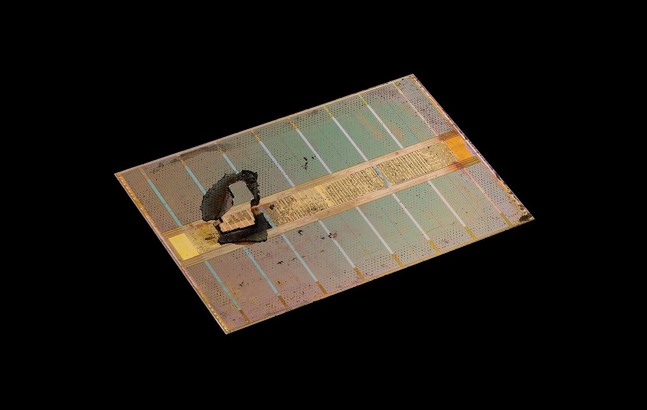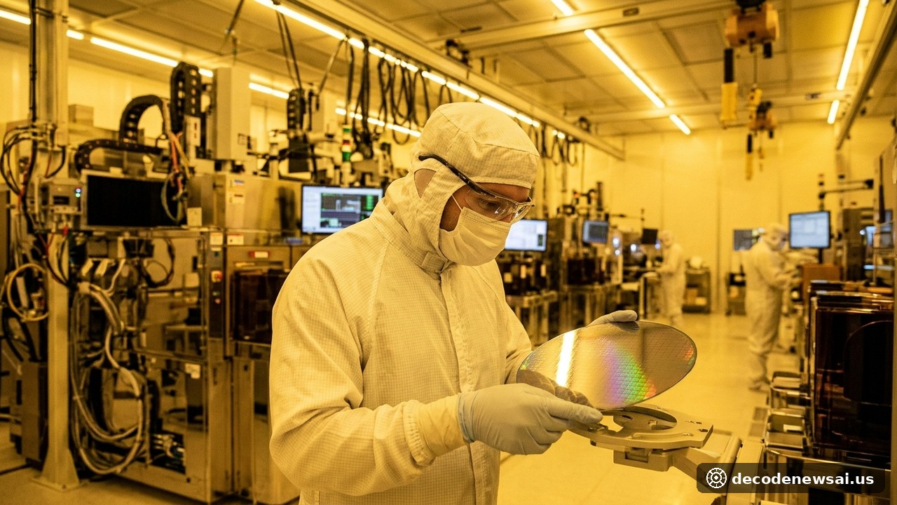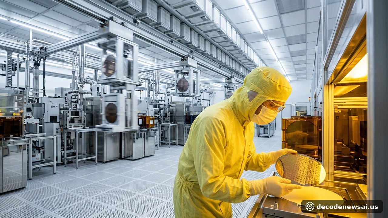
Taiwan Semiconductor Manufacturing Company (TSMC) has formally initiated a strategic feasibility assessment to evaluate manufacturing advanced three-dimensional dynamic random-access memory (3D DRAM) at the explicit request of its largest customer, Nvidia Corporation. Multiple semiconductor industry reports confirmed on November 6, 2026, that the evaluation is led by TSMC Vice President Hsu Kuo-chin, a former Micron Technology engineering executive who currently oversees TSMC's advanced packaging division. The strategic study represents TSMC's first exploratory step beyond its traditional pure-play logic foundry mandate, aiming to dismantle the global supply monopoly currently held by South Korean memory incumbents.
Technical Baseline and Strategic Metrics Governing TSMC's 3D DRAM Evaluation
- Requesting Anchor Customer: Nvidia Corporation (premier AI computing client)
- Lead Technical Evaluation Director: VP Hsu Kuo-chin (Advanced Packaging & Systems)
- Bandwidth Scaling Target for Next-Gen GPUs: 3x to 5x throughput leap exceeding TB/s boundaries
- High-Performance Computing (HPC) Revenue Share: 68.0% of total consolidated Q3 2026 foundry revenue
Why Did Nvidia Strongly Urge TSMC to Enter Memory Chip Manufacturing?
The impetus behind Nvidia's aggressive lobbying stems from acute technical friction surrounding the "memory wall." As artificial intelligence foundation models expand into trillions of parameters utilizing sparse mixture-of-experts architectures, raw GPU floating-point throughput is no longer the sole computational bottleneck. The staggering latency and thermodynamic energy dissipated while transporting data between processing cores and external high-bandwidth memory (HBM) stacks have emerged as the paramount architectural constraint crippling next-generation AI cluster scaling.
At present, the global merchant high-bandwidth memory market is almost entirely controlled by a duopoly comprising SK Hynix and Samsung Electronics. Beyond exerting intense commercial pricing leverage, existing HBM manufacturing depends on mechanically grinding down conventional 2D DRAM wafers and stacking them via through-silicon vias (TSVs) and micro-bumps—a complex assembly method facing severe thermal dissipation limits and yield degradation. Nvidia Chief Executive Officer Jensen Huang requires a disruptive, native 3D DRAM topology that stacks memory cells vertically directly on silicon, designed from inception to integrate seamlessly with TSMC's proprietary Chip-on-Wafer-on-Substrate (CoWoS) packaging to bypass traditional memory supply chains.
What Engineering Pathways Are Under Internal Review by TSMC Leadership?
Renowned for rigorous capital expenditure discipline, TSMC executive management is approaching the capital-intensive and historically volatile memory sector with calculated prudence. The internal task force commanded by Hsu Kuo-chin is scrutinizing two operational implementation roadmaps: constructing a dedicated, cleanfield greenfield 3D DRAM pilot fab within Taiwan's science parks, or executing an acquisition of an existing legacy specialty DRAM facility and retrofitting the cleanroom lines with advanced extreme ultraviolet (EUV) lithography tools to accelerate time-to-market.
Seismic Disruption Across the Global Semiconductor and AI Compute Landscape
Should TSMC officially sanction volume commercialization of custom 3D DRAM for Nvidia, the move will permanently obliterate the forty-year-old operational boundary separating Taiwan's logic foundry ecosystem from South Korea's memory domain. The entrenched HBM moats cultivated by Samsung and SK Hynix would confront direct, existential competition from the world's most advanced semiconductor manufacturing powerhouse. Furthermore, global technology enterprises reliant on TSMC would gain access to a unified, vertically integrated foundry capable of fabricating compute, memory, and packaging within a single sovereign ecosystem.
While TSMC and Nvidia have both refrained from public comment, capital markets have registered the profound strategic gravity of the initiative. In the hyper-competitive arena of frontier artificial intelligence, commercial leadership is no longer determined solely by circuit architecture, but by three-dimensional physical integration. TSMC's exploratory foray into 3D DRAM redefines the foundational boundaries of computing, setting the stage for the next decade of sovereign infrastructure supporting artificial general intelligence.